In chip manufacturing, there are three core links, which are thin film deposition, photolithography, and etching.
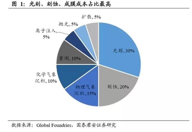
Among them, lithography is the most complex, critical, costly, and time-consuming link; the cost of etching is second only As for photolithography, the importance is also rising; and thin film deposition is also an indispensable important process. In manufacturing, in order to realize the layered structure of large-scale integrated circuits, it is necessary to repeat the process of deposition-etching-deposition.
From the figure below, we can also see the important position of etching in chip manufacturing.

Engraving The etching can be divided into two technical schemes: wet etching and dry etching.
The so-called wet etching is easy to understand. It is to use liquid chemical reagents to corrode and digest the surface of the wafer. We need to remove Texture pattern.
Dry etching, obviously, it is not a liquid such as a chemical reagent, it uses energy Beams, such as ion beams, electron beams, laser beams, etc.
At present, the most commonly used is ion beam, to be precise, plasma, which hits the surface of the wafer. It produces a chemical reaction or a physical reaction (or both chemical and physical reactions) with the wafer to achieve the purpose of etching.
At present, the mainstream solution used in the etching machine field is dry etching, which accounts for at least 90%.
This is mainly because there are some defects in wet etching.
First of all, wet etching requires a large amount of corrosive chemical reagents harmful to the human body and the environment, so in large-scale integrated circuits In manufacturing, it is gradually being eliminated.
Secondly, wet etching has an isotropic problem, which means that because wet etching uses The chemical reagent is a liquid, so the directionality is not well controlled when the chemical reaction is carried out. During etching, the peripheral part of the bottom of the pattern may also be reacted or even hollowed out. This is not what people want to see.
Because of this problem, wet etching is difficult to use in sub-micron (less than 1μm) semiconductors , Dry etching must be used.
The dry etching has high accuracy and no contaminants. In short, it is more advanced.


